Phone:86-0714-3056766 E-mail:sukie@hbzpdz.com
Solving dewetting in conformal coating
What is conformal coating ?
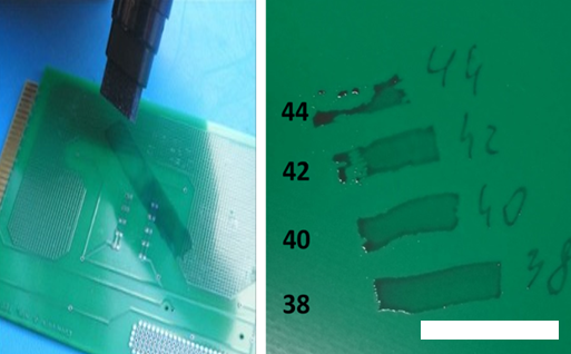
IPC T-50 defines It is an insulating protective covering that conforms to the configuration of the objects coated, providing a protective barrier against deleterious effects from environmental conditions. Some photos to let you know conformal coating.
Why use conformal coating ?
Conformal coating provides advantages
× Inhibit current leakage due to environmental contamination
× prevent PCBA from corrosion
× Improve fatigue resistance of solder joints
× Inhibit arcing, corona discharge, Tin whisker, etc.
× Provide mechanical support and vibration resistance
× Provide resistance to fluids and humidity,printed circuit board
These advantages ensure the reliability of products under specific conditions, for a specified period of time, without failure.
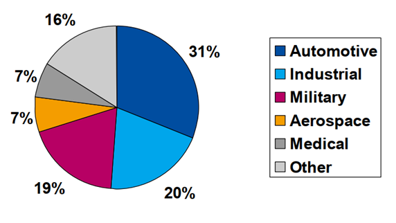
The typical defects of applying conformal coating
When we apply conformal coating as protection for PCBA, we may meet the typical problems in below drawing, we focus on De-wetting this time.
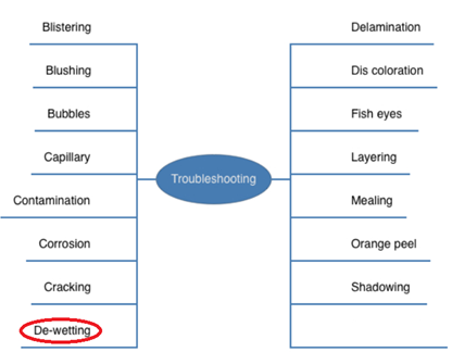
What is de-wetting in conformal coating ?
De-wetting is the tendency of the coating material to refuse to wet the PCB surface that it has been applied to evenly, refer to below photo.
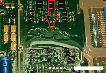
It will cause the PCBA can not be protected as the design purpose.
What cause de-wetting in conformal coating?
Below factors can cause de-wetting in conformal coating
× improper solder mask
× Residues from board manufacture including silicone surfactants.
× Oil or contamination in handling process.
× Cleaning bath contamination where rinsing has failed
× Soldering process
How to avoid de-wetting in conformal coating ?
Step 1. Solder mask selection
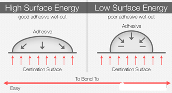
Higher surface energy of solder mask should be selected when conformal coating will be applied on PCBA. The surface energy of the solder mask should be higher than surface tension of the conformal coating, or you will observe de-wetting.printed circuit board
The PCB user should specify a minimum level of surface tension in specification, typical >=38dyne/cm2 is required.
PCB manufacturer has to recognize the term of solder mask surface tension and select right solder mask before PCB production.
Step 2. Process control
×Minimize the contaminants that are on the component parts before assembly. This includes laminate & component cleanliness control before assembly and selection of low residue process materials including fluxes and pastes.printed circuit board
×Removal of silicone compounds near conformal coating areas. These include silicone conformal coatings and lubrication sprays, greases, oils, etc.
×Reflow process optimization for complete activation of flux and minimization of flux active residues.
Step 3. Cleaning the boards before coating
Cleanliness of the boards before conformal coating will minimize de-wetting defects, the typical cleaning includes
Simple DI wash to remove minor water soluble residues and dust.
Saponifier assisted wash to remove tougher residues such as flux, oils and stains
Plasma treatment to remove wash resistant stains and to activate the surface with very high surface energy. Plasma can be taken as reworking solution when solder mask applied on PCB are not compatible with conformal coating.
Notes: Testing of surface energy after each assembly process is recommended.
How to get the surface energy of solder mask ?
Measuring PCB surface energy with Dyne pens
It is a simple test and easy to do with the right set of Dyne Pens. We can use the pen to check the incoming cleanliness quality of printed circuit boards where a problem is suspected and if the right solder mask is applied on PCB.
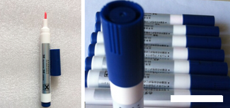
Here are a few steps on how to measure surface energy
•Make sure your dyne pens are not contaminated or outdated.
•Make sure your dyne pens are stored at room temperature.
•Before testing, make sure the PCB is clean and free from damage.
•Remove the pen cap and make sure that the pen tip is saturated. With light pressure, draw 3-4 parallel lines with the dyne pen onto the test area of your PCB. Keep note of the time between when the solution is applied to the substrate until when the solution beads up or begins to shrink (stays wet). If the solution does not shrink after 3 seconds, repeat the test with the next highest dyne pen. If the solution breaks into droplet in less than 3 seconds, repeat test with next lowest dyne pen. If the ink holds for one to three seconds before losing its integrity, the dyne level of the marker closely matches that of the sample.
Refer to some pictures about the surface energy test results
